Scanning electron microscopy

The scanning electron microscope (SEM) is a type of electron microscope that creates various images by focusing a high energy beam of electrons onto the surface of a sample and detecting signals from the interaction of the incident electrons with the sample's surface. The type of signals gathered in a SEM varies and can include secondary electrons, characteristic x-rays, and back scattered electrons. In a SEM, these signals come not only from the primary beam impinging upon the sample, but from other interactions within the sample near the surface. The SEM is capable of producing high-resolution images of a sample surface in its primary use mode, secondary electron imaging. Due to the manner in which this image is created, SEM images have great depth of field yielding a characteristic three-dimensional appearance useful for understanding the surface structure of a sample. This great depth of field and the wide range of magnifications are the most familiar imaging mode for specimens in the SEM. Characteristic x-rays are emitted when the primary beam causes the ejection of inner shell electrons from the sample and are used to tell the elemental composition of the sample. The back-scattered electrons emitted from the sample may be used alone to form an image or in conjunction with the characteristic x-rays as atomic number contrast clues to the elemental composition of the sample.
History
The SEM was pioneered by Manfred von Ardenne in the 1930s [1] [2]. The instrument was further developed by Charles Oatley and first commercialized by Cambridge Instruments.
Scanning process
In a typical SEM, electrons are thermionically emitted from a tungsten or lanthanum hexaboride (LaB6) cathode and are accelerated towards an anode; alternatively, electrons can be emitted via field emission (FE). Tungsten is used because it has the highest melting point and lowest vapour pressure of all metals, thereby allowing it to be heated for electron emission. The electron beam, which typically has an energy ranging from a few hundred eV to 100 keV, is focused by one or two condenser lenses into a beam with a very fine focal spot sized 0.4 nm to 5 nm. The beam passes through pairs of scanning coils or pairs of deflector plates in the electron optical column, typically in the objective lens, which deflect the beam horizontally and vertically so that it scans in a raster fashion over a rectangular area of the sample surface. When the primary electron beam interacts with the sample, the electrons lose energy by repeated scattering and absorption within a teardrop-shaped volume of the specimen known as the interaction volume, which extends from less than 100 nm to around 5 µm into the surface. The size of the interaction volume depends on the electrons' landing energy, the atomic number of the specimen and the specimen's density. The energy exchange between the electron beam and the sample results in the emission of electrons and electromagnetic radiation, which can be detected to produce an image, as described below.
Sample preparation
Metal specimens require no special preparation for SEM, except for trimming to appropriate size to fit in a specimen chamber, and make appropriate sectioning if necessary.
Nonconductive solid specimens should be coated with a layer of conductive material, except when observed with Variable Vacuum or Environmental SEM. An ultrathin coating of electrically-conducting material is deposited either by high vacuum evaporation or by low vacuum sputter coating of the sample. This is done to prevent the accumulation of static electric fields at the specimen due to the electron irradiation during imaging. Such coatings include gold, gold/palladium, platinum, tungsten, graphite etc. Another reason for coating, even when there is more than enough conductivity, is to improve contrast, a situation more common with the operation of a FESEM (field emission SEM).
Embedding in a resin with further polishing to a mirror-like finish could be beneficial for both biological and materials specimens, especially when imaging in backscattered electrons or X-ray microanalysis are performed.
A biological specimen requires fixation to preserve its structure, which is usually performed by incubation of specimen in solution of fixative, such as gluteraldehyde or formalin.
If not used in ESEM, biological specimen then should be dehydrated, usually by replacing water with organic solvents such as ethanol or acetone, and then removing solvents.
If SEM is equipped for cryo-microscopy, then cryofixation could be used. Cryofixation – freezing a specimen so fast, to liquid nitrogen or even liquid helium temperatures, that the water forms vitreous (non-crystalline) ice. This preserves the specimen in a snapshot of its solution state. An entire field called cryo-electron microscopy has branched from this technique. With the development of cryo-electron microscopy of vitreous sections (CEMOVIS), it is now possible to observe virtually any biological specimen close to its native state.
Another cryo-technique for biological specimens is cryo-fracture, when frozen specimen is fractured in special apparatus, sputter coated and transferred into SEM cryo-holder while still frozen.
Due to the loss of information, gold coating is often a semi-destructive process since removing a gold coating chemically requires aggressive chemicals like potassium cyanide or aqua regia.
Alternative techniques, for example the low-vacuum environmental SEM, allow samples to be imaged without such plating and without the loss of natural contrast arising from the beam-specimen interaction. Gold has a high atomic number and produces high topographic contrast and resolution but the information thus produced can obscure the underlying fine detail of the specimen under examination.
Detection of secondary electrons
The most common imaging mode monitors low energy (<50 eV) secondary electrons. Due to their low energy, these electrons originate within a few nanometers from the surface. The electrons are detected by an Everhart-Thornley detector which is a type of scintillator-photomultiplier device and the resulting signal is rendered into a two-dimensional intensity distribution that can be viewed and saved as a Digital image. This process relies on a raster-scanned primary beam. The brightness of the signal depends on the number of secondary electrons reaching the detector. If the beam enters the sample perpendicular to the surface, then the activated region is uniform about the axis of the beam and a certain number of electrons "escape" from within the sample. As the angle of incidence increases, the "escape" distance of one side of the beam will decrease, and more secondary electrons will be emitted. Thus steep surfaces and edges tend to be brighter than flat surfaces, which results in images with a well-defined, three-dimensional appearance. Using this technique, resolutions less than 1 nm are possible.
Detection of backscattered electrons
* backscattered electrons analysis - composition resolution
* secondary electrons analysis - relief
Backscattered electrons consist of high-energy electrons originating in the electron beam, that are reflected or back-scattered out of the specimen interaction volume. Backscattered electrons may be used to detect contrast between areas with different chemical compositions, especially when the average atomic number of the various regions is different, since the brightness of the BSE image tends to increase with the atomic number.
Backscattered electrons can also be used to form an electron backscatter diffraction (EBSD) image. This image can be used to determine the crystallographic structure of the specimen.
There are fewer backscattered electrons emitted from a sample than secondary electrons. The number of backscattered electrons leaving the sample surface upward might be significantly lower than those that follow trajectories toward the sides. Additionally, in contrast to the case with secondary electrons, the collection efficiency of backscattered electrons cannot be significantly improved by a positive bias common on Everhart-Thornley detectors. This detector positioned on one side of the sample has low collection efficiency for backscattered electrons due to small acceptance angles. The use of a dedicated backscattered electron detector above the sample in a "doughnut" type arrangement, with the electron beam passing through the hole of the doughnut, greatly increases the solid angle of collection and allows for the detection of more backscattered electrons.
Beam-injection analysis of semiconductors
The nature of the SEM's probe, energetic electrons, makes it uniquely suited to examining the optical and electronic properties of semiconductor materials. The high-energy electrons from the SEM beam will inject charge carriers into the semiconductor. Thus, beam electrons lose energy by promoting electrons from the valence band into the conduction band, leaving behind holes.
In a direct bandgap material, recombination of these electron-hole pairs will result in cathodoluminescence; if the sample contains an internal electric field, such as is present at a p-n junction, the SEM beam injection of carriers will cause electron beam induced current (EBIC) to flow.
Cathodoluminescence and EBIC are referred to as "beam-injection" techniques, and are very powerful probes of the optoelectronic behavior of semiconductors, particularly for studying nanoscale features and defects.
Cathodoluminescence
Cathodoluminescence, the emission of light when atoms excited by high-energy electrons return to their ground state, is analogous to UV-induced fluorescence, and some materials such as zinc sulphide and some fluorescent dyes, exhibit both phenomena. Cathodoluminescence is most commonly experienced in everyday life as the light emission from the inner surface of the cathode ray tube in television sets and computer CRT monitors. In the SEM, CL detectors either collect all light emitted by the specimen, or can analyse the wavelengths emitted by the specimen and display a spectrum or an image of the cathodoluminescence in real colour.
X-ray microanalysis
X-rays, which are also produced by the interaction of electrons with the sample, may also be detected in an SEM equipped for energy-dispersive X-ray spectroscopy or wavelength dispersive X-ray spectroscopy.
Resolution of the SEM
The spatial resolution of the SEM depends on the size of the electron spot, which in turn depends on both the wavelength of the electrons and the magnetic electron-optical system which produces the scanning beam. The resolution is also limited by the size of the interaction volume, or the extent to which the material interacts with the electron beam. The spot size and the interaction volume both might be large compared to the distances between atoms, so the resolution of the SEM is not high enough to image individual atoms, as is possible in the shorter wavelength (i.e. higher energy) transmission electron microscope (TEM). The SEM has compensating advantages, though, including the ability to image a comparatively large area of the specimen; the ability to image bulk materials (not just thin films or foils); and the variety of analytical modes available for measuring the composition and nature of the specimen. Depending on the instrument, the resolution can fall somewhere between less than 1 nm and 20 nm. In general, SEM images are easier to interpret than TEM images.
Environmental SEM
Conventional SEM requires samples to be imaged under vacuum, which means that samples that would produce a significant amount of vapour, e.g. biological samples, need to be either dried or cryogenically frozen. This means that processes involving transitions to or from liquids or gases, such as the drying of adhesives or melting of alloys, liquid transport, chemical reactions and solid-air-gas systems in general could not be observed.
The first commercial development of the Environmental SEM (ESEM) in the late 1980s [3] [4] allowed samples to be observed in low-pressure gaseous environments (e.g. 1-50 Torr) and high relative humidity (up to 100%). This was made possible by the development of a secondary-electron detector [5] [6] capable of operating in the presence of water vapour and by the use of pressure-limiting apertures with differential pumping in the path of the electron beam to separate the vacuum regions around the gun and lenses from the sample chamber.
The first commercial ESEMs were produced by the ElectroScan Corporation in USA in 1988 [7]. ElectroScan were later taken over by Philips (now FEI Company) in 1996 [8].
ESEM is especially useful for non-metallic and biological materials because coating with carbon or gold is unnecessary. Plastics and Elastomers can now be routinely examined, as can biological samples. Coating can be difficult to reverse, and may reduce the value of the results obtained. For example very small details on the surface of the sample may be concealed by the coating, let alone that coating is done under vacuum, which drastically alters hydrated specimens.
See also
| Wikimedia Commons has media related to Scanning electron microscopic images. |
References
- ↑ von Ardenne, Manfred (1938). "Das Elektronen-Rastermikroskop. Theoretische Grundlagen". Zeitschrift fur Physik (in German). 108: 553–572.
- ↑ von Ardenne, Manfred (1938). "Das Elektronen-Rastermikroskop. Praktische Ausführung". Z. Techn. Phys. (in German). 108: 407–416.
- ↑ Danilatos, G,D (1988). "Foundations of environmental scanning electron microscopy". Advances in Electronics and Electron Physics. 71: 109–250.
- ↑ US patent 4823006, Gerasimos D Danilatos, George C Lewis, "Integrated electron optical/differential pumping/imaging signal detection system for an environmental scanning electron microscope", issued 1989-4-18
- ↑ Danilatos, G,D (1990). "Theory of the Gaseous Detector Device in the ESEM". Advances in Electronics and Electron Physics. 78: 1–102.
- ↑ US patent 4785182, James F Mancuso, William B Maxwell, Gerasimos D Danilatos, "Secondary Electron Detector for Use in a Gaseous Atmosphere", issued 1988-11-15
- ↑ History of Electron Microscopy, 1980s
- ↑ History of Electron Microscopy 1990s
External links
General
- Notes on the SEM Notes covering all aspects of the SEM
History
- Microscopy History links from the University of Alabama Department of Biological Sciences
- The Early History and Development of SEM from Cambridge University Engineering Department
- Milestones in the History of Electron Microscopy from the Swiss Federal Institute of Zürich
- Environmental Scanning Electron Microscope (ESEM) history
Images
- Tescan Image Gallery Some great SEM images of various specimens, as well as analytical results
- Dennis Kunkel Microscopy, Inc. Large collection of SEM images - mostly false colour
- Jeol SEM Images Twelve SEM images of various specimens
- SEM Lab at the Smithsonian National Museum of Natural History; includes a gallery of images
- Rippel Electron Microscope Facility Many dozens of (mostly biological) SEM images from Dartmouth College.
Gallery of SEM images
The following are examples of images taken using a scanning electron microscope.
-
-
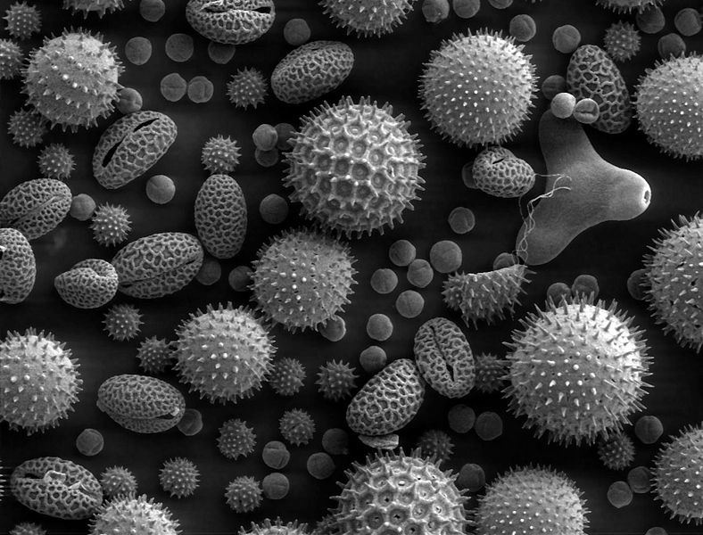
An SEM image of various types of pollen.
-
SEM Picture of a Diatom at magnification of 5000X.
-
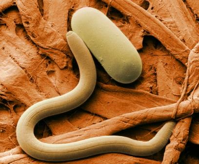
False coloured SEM image of soybean cyst nematode and egg.
-
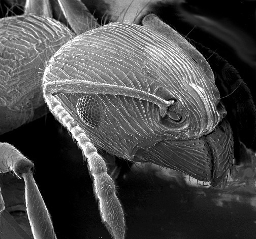
SEM image of an ant head.
-
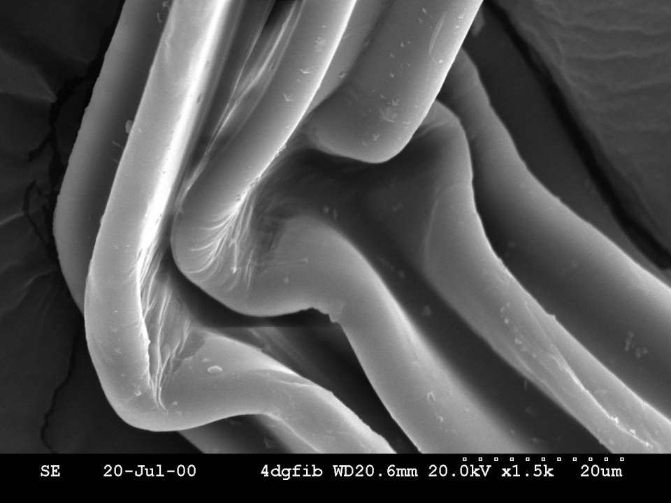
SEM image of asbestos fibers.
-
Compound eye of Antarctic krill Euphausia superba.
-
Ommatidia of Antarctic krill eye.
-
SEM image of a discharged nematocyst.
-
SEM image of the upper body of a Drosophila.
-
SEM images of the compound eye of a Drosophila.
-
SEM image of a cricket's spiracle valve.
-

SEM image of normal circulating human blood.
-
SEM image of a hederelloid from the Devonian of Michigan (largest tube diameter is 0.75 mm).
-
Backscattered Electron image of an Antimony rich region in a fragment of ancient glass.
-
SEM image of the corrosion layer on the surface of an ancient glass fragment, note the laminar structure of the corrosion layer.
-
SEM image of a photoresist layer used in semiconductor manufacturing


bg:Сканиращ eлектронен микроскоп cs:Rastrovací elektronový mikroskop de:Rasterelektronenmikroskop fa:میکروسکوپ الکترونی روبشی it:Microscopio elettronico a scansione nl:Rasterelektronenmicroscoop sl:Vrstični elektronski mikroskop uk:Скануючий електронний мікроскоп Template:WikiDoc Sources